Table Of Content
Some double layer PCBs have a ground layer, where the entire bottom layer is covered with a copper plane connected to ground. The positive traces are routed on top and connections to ground are made with through holes or vias. Ground layers are good for circuits that are prone to interference, because the large area of copper acts as a shield against electromagnetic fields. Before you start designing your PCB, it’s a good idea to make a schematic of your circuit.
Manually Creating a New Schematic Design Rule
Take a look at this article to see how you can set up a Net Class in Altium Designer. Effective heat distribution and cooling layout are crucial for high-power devices. Plan a reasonable heat dissipation layout to ensure efficient heat dissipation, preventing performance degradation or damage due to excessive temperatures. Distribute multiple high-power components strategically across the PCB to balance heat distribution throughout the board.
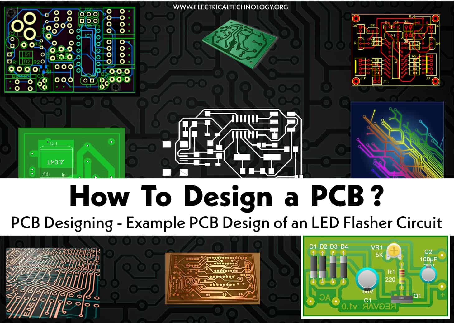
Getting Started with PCB Design
The most important thing you can do to ensure a smooth PCB manufacturing process and PCB assembly is to follow your manufacturer’s DFM guidelines. Contrary to what some believe, DFM is specific to your manufacturer. Reliance on default or general specifications can cause manufacturing delays and may require design changes. This is easily avoided by setting up your DRCs to match the capabilities of your manufacturer. When you need more resources to finish a complex design, Altium gives you free access to PCB design tutorials (both online and in-application) that guide you through the various design features.
Working with a Connection Object on a PCB in Altium Designer
But you might need to create your own footprint for some unusual components. Most EDA/ECADs have modules that can do this easily using dimensions from the device’s datasheet. In a star topology, multiple sub-circuits are directly connected to a central power supply.
A broader perspective on PCB design - Engineer Live
A broader perspective on PCB design.
Posted: Mon, 23 Oct 2023 07:00:00 GMT [source]
3) Click on the Bottom Layer tab at the bottom of the workspace to make it the current, or active layer, for routing. 3) Define the scope of the rule by setting the first dropdown menu to Net and the second dropdown menu to 12V. 3) Either click the New Rule button below the rule summary list or right-click and select New Rule from the context menu. 1) Open the PCB Rules and Constraints Editor by selecting Design » Rules from the toolbar.
#2 - Fine-Tuning Your Component Placement
While strict orthogonality may not always be feasible due to space limitations, it is sufficient to ensure that adjacent layer signals are not parallel. In circuit design, the 3W rule plays a crucial role as a key design criterion, encompassing the width of traces, the spacing between them, and the clearance between traces and surrounding areas on the board. Careful consideration of these parameters at an early stage is PCB design basics, and additionally requires strict adherence throughout the layout and trace process. Create electronic designs from schematic capture to final design documentation and manufacturing files – all in one intuitive interface and unified data model.
DFM reduces the need for manpower and eliminates the need for redesigns and iterations. With DFM processes, more products are able to be manufactured in a shorter span of time. Incorporating DFM aspects into PCB design provides alternative component choices, considering the availability of the original component selected. In this way, DFM processes decrease lead time and product time-to-market. When optimizing the product development process, one of the major areas to improve is the PCB layout design for manufacturing. Once your board has passed the final DRC, you need to generate the design files for your manufacturer.
Some of the important routes will include your power nets, any impedance-controlled nets, and any noise-sensitive nets like low-level analog signals. Be sure to utilize good routing guidelines and take advantage of Altium Designer tools to simplify the process, such as highlighting nets and interactive routing features. PCB design software and circuit design tools are primarily used by engineers to create printed circuit boards for use in a wide variety of consumer and commercial electronics.
Design for Manufacturing (DFM)
An example of connection lines that connect between different layers in a multi-layer board in single layer mode. In the ground plane layout, dividing the ground plane into digital and analog ground segments can effectively reduce interference between digital and analog signals. High-speed interfaces can benefit from a single-point connection that connects digital and analog grounds, eliminating potential ground loops between them.
Zuken Releases Host of Upgrades to Flagship PCB Design Software - News - All About Circuits
Zuken Releases Host of Upgrades to Flagship PCB Design Software - News.
Posted: Tue, 05 Sep 2023 07:00:00 GMT [source]
You can also migrate your PCB designs to OrCAD from other popular programs like Altium, Eagle, and PADS, with guides on how to do so for each different software. PADS even hosts a unique program that can provide eligible startups with discounted access to PADS Profesional, which is certainly worth considering if you have a young business that relies on layout PCB software. There’s also a forum where you can open discussions and interact with other users, and if you’re a programmer you can use the source code to help fix bugs and develop your own features. So if you’re looking for the best open source PCB software, Fritzing is the one for you.
Speed up layout design by involving more than one Engineer to design different parts of the same PCB simultaneously. See our Engineering Essentials page for a full list of cornerstone topics surrounding electrical engineering. Black, gray, red, and even yellow silkscreen colors are widely available; it is, however, uncommon to see more than one color on a single board.

Luckily, the top programs from our PCB design software list like Altium and OrCAD offer free trials, so you can use these to try them out before committing to hefty fees. Here are the key factors to consider when conducting a PCB design software comparison. The next step up is PADS Standard Plus, which comes with advanced layout capabilities as well as simulation and analysis tools.
However, your design decisions need to be manufacturable in standard processes, so a designer needs to be familiar with the limits of what can be fabricated in a PCB. The list of products below is based purely on reviews and profile completeness. There is no paid placement and analyst opinions do not influence their rankings. We are committed to ensuring information on our site is reliable, useful, and worthy of your trust. Have your computer with the PCB Design close by so that you can check the orientation and value of components if needed. If that’s not possible, print out the schematic with values and the board layout.
Unrouted connection lines between thepads of two placed board components. This is just a sample of the rules that can govern any PCB layout, but these rules are designed to help ensure a board is manufacturable at the required scale with your fabricator's standard capabilities. These rules can be applied to individual objects or to groups of objects using queries or using Net Class objects.
The DFM process checks the accuracy of the design at the system level, sub-system level, and component level. These all-level process checks ensure the design is optimized and cost-effective. Impedance matching becomes critical when the delay time of PCB wiring exceeds 1/4 of the signal rise time or fall time, effectively making the wiring act as a transmission line. To ensure accurate signal transmission, various impedance matching methods can be employed based on the network connection mode and wiring topology. In circuits, reflections can occur when transmission speeds are high, which can negatively impact signal quality. To avoid such situations, it is essential to keep the wiring width of the same network consistent.


No comments:
Post a Comment